8.8 KiB
ECE 240: Electronic Circuits
Diodes
A diode is a two-terminal device that only allows current to flow in the direction of the arrow.
 (Source:
Wikimedia Commons)
(Source:
Wikimedia Commons)
The current across a diode is, where is a forced saturation current, is the voltage drop across it, and is the thermal voltage such that , where is the temperature, is the Boltzmann constant, and is the charge of an electron:
!!! tip - \(V_T\approx\pu{25 mV}\) at 20°C - \(V_T\approx\pu{20 mV}\) at 25°C
A diode is open when current is flowing reverse the desired direction, resulting in zero current, until the voltage drop becomes so great that it reaches the breakdown voltage . Otherwise, the above current formula is followed.
 (Source:
Wikimedia Commons)
(Source:
Wikimedia Commons)
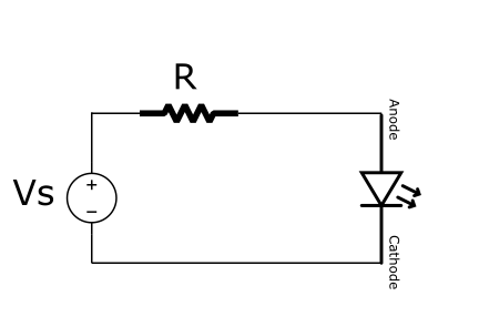
Diodes are commonly used in rectifier circuits — circuits that convert AC to DC.
By preventing negative voltage, a relatively constant positive DC voltage is obtained. The slight dip between each hill is known as ripple .
 (Source:
Wikimedia Commons)
(Source:
Wikimedia Commons)
In a simple series RC circuit, across a diode, Where , and :
Zener diodes
A Zener diode is a calibrated diode with a known breakdown voltage, . If the voltage across the diode would be greater than , it is capped at .
 (Source:
Wikimedia Commons)
(Source:
Wikimedia Commons)
Voltage/current biasing
Solving for current for each element in a series returns a negative linear line and other non-linear lines.
- the linear line is the load line, which represents the possible solutions to the circuit when it is loaded
- Depending on the base current , the diode or transistor will be biased toward one of the curves, and the voltage and current will settle on one of the intersections, or bias points.
 (Source:
Wikimedia Commons)
(Source:
Wikimedia Commons)
- To bias current, as (or, in practical terms, ), the slope of the load line , which results in a constant current.
- To bias voltage, as , the slope of the load line , which results in a constant voltage.
!!! example
The current across the resistor and the diode is the same:

\begin{align*}
i_D&=\frac{V_s}{R} \\
i_D&\approx I_se^{V_D/V_T}
\end{align*}
If a diode is put in series with AC and DC voltage sources and :
\[\begin{align*} i_D(t)&=I_se^{(V_D+V_d(t))/V_T} \\ &=\underbrace{I_se^{V_D/V_T}}_\text{bias current}\ \underbrace{e^{V_d(t)/V_T}}_\text{$\approx 1+\frac{V_d}{V_T}$} \\ &=I_D\left(1+\frac{V_d}{V_T}\right) \\ &=\underbrace{I_D}_\text{large signal = bias = DC}+\underbrace{I_D\frac{V_d(t)}{V_T}}_\text{small signal = AC} \end{align*}\]
Diodes may act as resistors, depending on the bias current. They may exhibit a differential resistance:
!!! example Thus from the previous sequence:
$$i_D(t)=I_D+\frac{1}{r_d}V_d(t)$$Signal analysis
- Analyse DC signals
- assume blocking capacitors are open circuits
- turn off AC sources
- Analyse AC signals
- assume blocking capacitors are shorts
- turn off DC sources
- replace diode with effective resistor (the differential resistor)
!!! tip Most s in the circuit can be assumed to be significantly greater than , so can be removed in series or can be removed in parallel.
!!! warning Oftentimes, turning off a DC source to nowhere is actually a short to ground.
MOSFETs
A MOSFET is a transistor. Current flows from the drain to the source, and only if voltage is applied to the gate.
 (Source:
Wikimedia Commons)
(Source:
Wikimedia Commons)
![]() (Source:
Wikimedia Commons)
(Source:
Wikimedia Commons)
In strictly DC, current passes the gate if the gate voltage is greater than the threshold voltage . The difference between the two is known as the overdrive voltage :
At a small , or in AC, the slope of to is proportional to . The channel transconductance represents this slope, which is constant based on the transconductance parameter of the device.
Before the saturation region, the current grows exponentially:
Afterward, it remains constant, based on the overdrive voltage:
Common-source amplifiers
 (Source:
Wikimedia Commons)
(Source:
Wikimedia Commons)
Where :
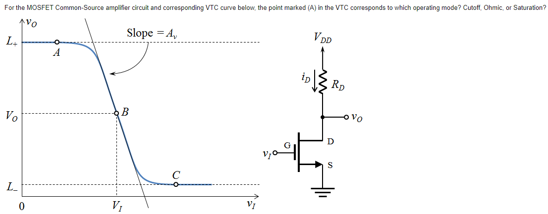
indicates AC voltage gain.
The gain can be modelled with Ohm’s law:
At a certain gate voltage:
\[\begin{align*} A_V&=\frac{\partial V_{DS}}{\partial V_{GS}} \\ &=-g_{DS}R_D \end{align*}\]
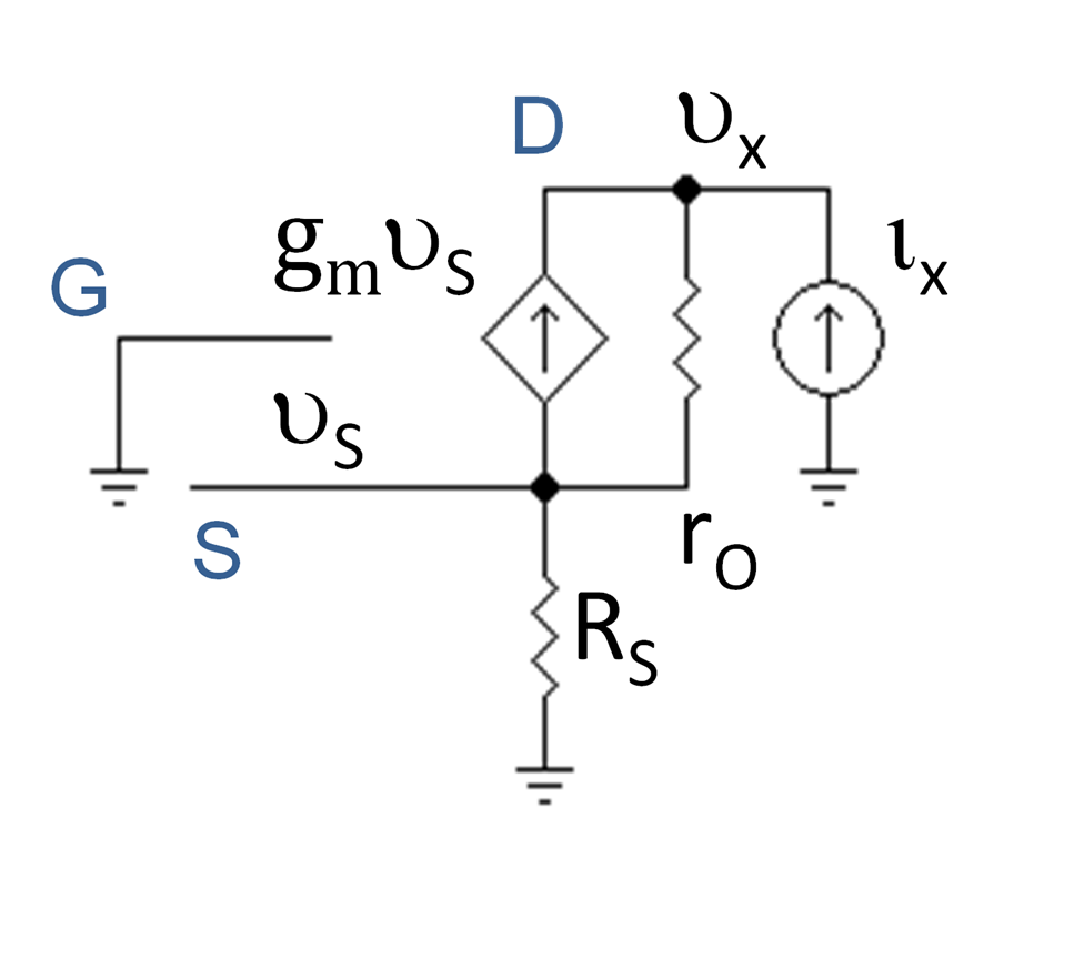
Small signal analysis
The current from the drain to the source is equal to:
For small signals, a transistor is equivalent to, where :

It can be assumed that the differential resistance is always significantly smaller than any other external resistance: .
To solve for the output resistance of the amplifier, turn off all sources and take the Thevenin resistance .
Common-drain amplifiers / source followers
The input resistance of common amplifiers is infinity.
 (Source:
Wikimedia Commons)
(Source:
Wikimedia Commons)
As is not necessarily zero, dependent sources must be left in when solving for output resistance, and so a small test source at the point of interest is required.
Common-gate amplifiers
These can be represented by either the T-model or pi-model. The gate of the transistor is grounded.

Differential pairs
These are used at the input of opamps.
In differential mode, assuming :
, so the current going down from both gates is equal . This means that node before is effectively ground, so the circuit can be split into two common source circuits.

In common mode:
The common-mode rejection ratio is:
MOSFET biasing
To bias a MOSFET:
- the transistor must be on:
- the transistor must be saturated
This is a negative feedback loop that forces a constant .
With two DC supplies (), having an results in:
PMOS transistors
These have current flowing from the source to the drain. It is effectively equal to an NMOS at all points but with its polarity reversed.
\[\begin{align*} \tag{triode}I_D&=k_p\left(|V_{ov}|-\frac 1 2V_{SD}\right)V_{SD} \\ \tag{saturation}I_D&=\frac 1 2 k_p(V_{SG}-|V_{tp}|)^2 \end{align*}\]
Frequency dependence
A parasitic capacitor from the gate to the source of an NMOS limits the bandwidth (gain). These represent physical limitations of electrodes. At the output, the current through the capacitor can be neglected. At the input, the current through the capacitor dominates.